


Memoria resistiva de acceso aleatorio (RRAM):descripción general de materiales, mecanismo de conmutación, rendimiento, almacenamiento de celdas multinivel (mlc), modelado y aplicaciones
Resumen
En este manuscrito, el progreso reciente en el área de la tecnología de memoria resistiva de acceso aleatorio (RRAM), que se considera una de las tecnologías de memoria emergentes más destacadas debido a su alta velocidad, bajo costo, densidad de almacenamiento mejorada, aplicaciones potenciales en varios campos y excelente La escalabilidad se revisa exhaustivamente. En primer lugar, se proporciona una breve descripción del campo de las tecnologías de memoria emergentes. Se discuten las propiedades del material, el mecanismo de conmutación de resistencia y las características eléctricas de RRAM. Además, se elaboran varios aspectos como la resistencia, la retención, la uniformidad y el efecto de la temperatura de funcionamiento y el ruido telegráfico aleatorio (RTN). Se presenta una discusión sobre la capacidad de almacenamiento de celdas multinivel (MLC) de RRAM, que es atractiva para lograr una mayor densidad de almacenamiento y un bajo costo. Se han proporcionado diferentes esquemas de operación para lograr una operación MLC confiable junto con sus mecanismos físicos. Además, en este trabajo se cubre una descripción detallada de las metodologías de conmutación y las relaciones de voltaje de corriente para varios modelos populares de RRAM. Se abordan brevemente las posibles aplicaciones de RRAM a varios campos como la seguridad, la computación neuromórfica y los sistemas lógicos no volátiles. El presente artículo de revisión concluye con la discusión sobre los desafíos y las perspectivas futuras de la RRAM.
Introducción
La memoria de acceso aleatorio denominada RAM puede ser volátil o no volátil. Una memoria volátil pierde sus datos almacenados previamente al quitar la fuente de alimentación, como es el caso de la memoria dinámica de acceso aleatorio (DRAM) y la memoria estática de acceso aleatorio (SRAM). En el caso de la memoria no volátil, los contenidos que se almacenaron anteriormente seguirán retenidos incluso después de la eliminación del suministro. La memoria flash es un ejemplo típico de memoria no volátil. Las tecnologías de memoria combinan las ventajas y desventajas para lograr un mayor rendimiento, p. Ej. Las DRAM empleadas en un sistema informático tienen alta capacidad y densidad, pero son volátiles, lo que significa que es necesario actualizarlas cada pocos milisegundos. Debido a esta actualización, el consumo de energía del dispositivo aumenta, lo que no es deseable. La SRAM, por otro lado, es rápida pero también volátil al igual que la DRAM; Además, las celdas SRAM son de mayor tamaño lo que dificulta su implementación a gran escala. La memoria flash, que consiste esencialmente en un transistor de efecto de campo semiconductor de óxido metálico (MOSFET) además de una puerta flotante en cada celda de memoria, se está utilizando actualmente de manera extensiva, particularmente para las aplicaciones integradas debido a su bajo costo y alta densidad. . Dependiendo de cómo estén organizadas las celdas de memoria, la memoria Flash se clasifica como NOR Flash y NAND Flash [1]. En NOR Flash, las celdas se leen y programan individualmente ya que están conectadas en paralelo a las líneas de bits. Esto se asemeja a la conexión en paralelo de transistores en una arquitectura de puerta CMOS NOR. Para el caso de NAND Flash, la arquitectura se asemeja a la de una puerta CMOS NAND ya que las celdas están conectadas en serie a las líneas de bits. Debe tenerse en cuenta que la conexión en serie consume menos espacio en comparación con la conexión en paralelo, lo que se traduce en un costo reducido de NAND Flash. Sin embargo, ambos tipos de memorias Flash adolecen de varias desventajas, como baja velocidad de operación (tiempo de escritura / borrado:1 ms / 0,1 ms), resistencia limitada (10 6 ciclos de escritura / borrado) y alto voltaje de escritura (> 10 V) [2].
Las tecnologías de memoria mencionadas anteriormente, es decir, DRAM, SRAM y Flash, son memorias basadas en almacenamiento de carga. DRAM almacena la información en forma de carga en el condensador, y SRAM se basa en el almacenamiento de carga en los nodos de los inversores de acoplamiento cruzado, mientras que la tecnología de memoria Flash utiliza la puerta flotante del transistor para almacenar la carga. Todas estas tecnologías de memoria basadas en almacenamiento de carga existentes se enfrentan actualmente a desafíos para escalar a un nodo de 10 nm o más. Esto se atribuye a la pérdida de carga almacenada a nanoescala, que da como resultado la degradación del rendimiento, la fiabilidad y el margen de ruido. Además, los requisitos de gran potencia dinámica de actualización para DRAM y potencia de fuga tanto para SRAM como para DRAM plantean serios desafíos para el diseño de la jerarquía de memoria futura.
Por lo tanto, actualmente se está desarrollando una nueva clase de memorias a las que generalmente se hace referencia como tecnologías de memoria emergentes y se están investigando activamente principalmente en la industria con el objetivo de revolucionar la jerarquía de memoria existente [3]. Estas tecnologías de memoria emergentes tienen como objetivo integrar la velocidad de conmutación de SRAM, la densidad de almacenamiento comparable a la de DRAM y la no volatilidad de la memoria Flash, por lo que se convierten en alternativas muy atractivas para la jerarquía de memoria futura.
Para clasificar un dispositivo de memoria como ideal, debe tener las siguientes características:voltaje de funcionamiento bajo (<1 V), resistencia de ciclo largo (> 10 17 ciclos), tiempo de retención de datos mejorado (> 10 años), bajo consumo de energía (fJ / bit) y escalabilidad superior (<10 nm) [4]. Sin embargo, no hay un recuerdo único hasta la fecha que satisfaga estas características ideales. Se están investigando activamente varias tecnologías de memoria emergentes para satisfacer una parte de estas características ideales de la memoria. Estas tecnologías de memoria que dependen del cambio de resistencia en lugar de la carga para almacenar la información son las siguientes:(i) memoria de cambio de fase (PCM), (ii) memoria de acceso aleatorio magnetorresistiva de par de transferencia de giro (STT-MRAM) y ( iii) memoria resistiva de acceso aleatorio (RRAM). En la memoria de cambio de fase, el medio de conmutación consiste en un material calcogenuro (comúnmente Ge 2 -Sb 2 -Te 5 , GST) [5-7]. PCM se basa en la diferencia de resistencia entre la fase cristalina y la fase amorfa para una capacidad de almacenamiento de datos eficiente. La fase cristalina denota el estado de baja resistencia (LRS) o el estado ON del dispositivo, mientras que la fase amorfa denota el estado de alta resistencia (HRS) o el estado OFF. La operación SET corresponde a LRS generalmente referida al almacenamiento de valor lógico "1", mientras que la operación RESET corresponde a HRS almacenando valor lógico "0" en el dispositivo. Para la operación SET, el PCM se calienta por encima de su temperatura de cristalización en la aplicación de pulso de voltaje, mientras que para la operación RESET, una corriente eléctrica más grande pasa a través de la celda y luego se corta abruptamente para derretir y luego enfriar el material con el fin de alcanzar el estado amorfo.
En la memoria de acceso aleatorio magnetorresistiva de par de transferencia de espín, la capacidad de almacenamiento se debe a la unión de tunelización magnética (MJT) [8-10], que consta de dos capas ferromagnéticas y un dieléctrico de tunelización intercalado entre ellas. La dirección magnética de la capa de referencia es fija, mientras que la aplicación de un campo electromagnético externo puede cambiar la dirección magnética de la capa ferromagnética libre. Si la capa de referencia y la capa libre tienen la misma dirección de magnetización, se dice que el MTJ está en el LRS. Para MTJ, al estar en el HRS, la dirección de magnetización de dos capas ferromagnéticas es antiparalela. RRAM consiste en una capa aislante (I) intercalada entre los dos electrodos metálicos (M) [11, 12]. RRAM se basa en la formación y ruptura de filamentos conductores correspondientes a LRS y HRS, respectivamente, en el aislante entre dos electrodos [13-15].
En la Tabla 1 se muestra una comparación detallada de las tecnologías de memoria existentes y emergentes. Como se desprende de la tabla, STT-MRAM y PCM tienen las ventajas de un área más pequeña en comparación con la de SRAM. Mientras que STT-MRAM ofrece una velocidad de escritura / lectura rápida, larga duración y bajo voltaje de programación, por otro lado, PCM tiene la desventaja de una extensa latencia de escritura. RRAM tiene un voltaje de programación más bajo y una velocidad de escritura / lectura más rápida en comparación con Flash y se considera como un reemplazo potencial de la memoria Flash. Entre todos los candidatos a la tecnología de memoria emergente, RRAM tiene ventajas significativas como fácil fabricación, estructura simple de metal-aislante-metal (MIM), excelente escalabilidad, velocidad de nanosegundos, larga retención de datos y compatibilidad con la tecnología CMOS actual, ofreciendo así un competitivo solución para la memoria digital futura [16]. Las ventajas más significativas de RRAM se muestran en la Fig. 1.
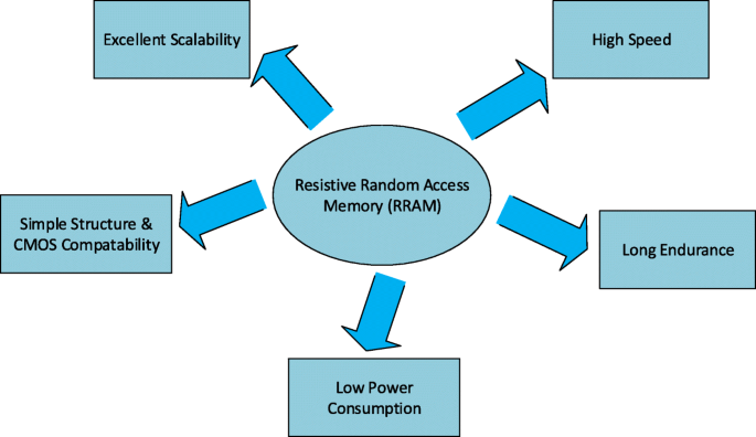
Ventajas de RRAM
En este trabajo, se presentan los avances recientes y una descripción detallada de la tecnología RRAM. En la sección “Memoria resistiva de acceso aleatorio (RRAM)” se analiza una revisión de los materiales de conmutación junto con la clasificación de los modos de conmutación y los detalles del mecanismo de conmutación. La sección "Métricas de rendimiento de la memoria resistiva de acceso aleatorio (RRAM)" destaca varias métricas de rendimiento de RRAM. Las características de la celda multinivel (MLC) de RRAM junto con varios esquemas de operación MLC y sus mecanismos físicos se analizan en la sección “Memoria de acceso aleatorio resistiva multinivel (RRAM)”. En la sección "Modelado de dispositivos RRAM" se presenta una discusión detallada sobre el modelado de dispositivos RRAM. En la sección “Aplicaciones de RRAM” se discuten varias aplicaciones de RRAM. Finalmente, los desafíos y las perspectivas de futuro de RRAM se presentan en la sección "Desafíos y perspectivas de futuro". La distribución por categorías de los artículos consultados en la preparación de este manuscrito de revisión se presenta en la Figura 2.
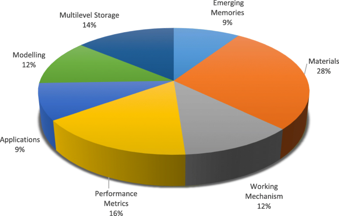
Distribución por categorías de los artículos consultados para la preparación de la revisión sobre RRAM
Memoria resistiva de acceso aleatorio (RRAM)
Materiales de conmutación de resistencia
Se ha observado que en algunos aisladores, el cambio de resistencia ocurre bajo la aplicación del campo eléctrico aplicado. Esta propiedad de cambio de resistencia se ha investigado recientemente para desarrollar futuras memorias no volátiles [17]. El fenómeno de conmutación por resistencia se ha observado en una variedad de óxidos, pero los óxidos metálicos binarios se han estudiado ampliamente como un material de conmutación preferido para futuras aplicaciones de memoria no volátil principalmente debido a su compatibilidad con el procesamiento CMOS BEOL. Varios materiales a base de óxidos metálicos que exhiben la resistencia al cambio no volátil, como el óxido de hafnio (HfO x ) [18-23], óxido de titanio (TiO x ) [24-31], óxido de tantalio (TaO x ) [32-36], óxido de níquel (NiO) [37-40], óxido de zinc (ZnO) [41-46], titanato de zinc (Zn 2 TiO 4 ) [47], óxido de manganeso (MnO x ) [48, 49], óxido de magnesio (MgO) [50], óxido de aluminio (AlO x ) [51-53] y dióxido de circonio (ZrO 2 ) [54–58] han atraído la mayor atención y se han estudiado ampliamente durante los últimos años. Estos óxidos metálicos se depositan generalmente mediante deposición por láser de pulso (PLD), deposición de capa atómica (ALD) y pulverización catódica reactiva. Sin embargo, ALD es un método ampliamente preferido debido a su capacidad para controlar con precisión el grosor y la uniformidad de la película delgada [59].
En los dispositivos electrónicos convencionales, la elección del material de los electrodos es importante, ya que actúan como rutas de transporte para los portadores. Para RRAM, la elección del material del electrodo afecta en gran medida el comportamiento de conmutación del dispositivo. Por ejemplo, en la estructura de cobre / poli (3-hexiltiofeno):éster metílico del ácido [6,6] -fenil-C61-butírico / óxido de indio-estaño (Cu / P3HT:PCBM / ITO), se observó un comportamiento de conmutación resistiva estable; sin embargo, desapareció después de que el electrodo de Cu fuera reemplazado por un electrodo de Pt [60]. Se ha utilizado una amplia variedad de materiales como electrodos para RRAM. Los materiales de los electrodos se pueden agrupar en cinco categorías en función de su composición, incluidos electrodos de sustancia elemental, electrodos a base de silicio, electrodos de aleación, electrodos de óxido y electrodos a base de nitrito. Los electrodos más abundantes y de uso común son electrodos de sustancias elementales que incluyen Al [51], Ti [49], Cu [30], grafeno [61], nanotubos de carbono [62], Ag [41], W [36], y Pt [44]. Para los electrodos a base de silicio, los únicos tipos de electrodos utilizados son Si de tipo p y Si de tipo n [63]. Los electrodos de aleación generalmente estabilizan el comportamiento de conmutación resistiva e incluyen principalmente Cu-Ti [64], Cu-Te [65] y Pt-Al [66]. Los electrodos de nitruro más comunes son TiN y TaN [67, 68]. Los electrodos a base de óxido son relativamente abundantes, incluidos ZnO dopado con Al [69], ZnO dopado con Ga [70] e ITO [71].
La lista de materiales de óxido metálico que se han utilizado recientemente en la fabricación del dispositivo RRAM junto con varias combinaciones de materiales utilizados para el electrodo superior y el electrodo inferior se muestran en la Tabla 2. También se presenta una comparación detallada de los diversos parámetros. A partir de la amplia variedad de materiales utilizados, se puede predecir que el cambio de resistencia no volátil se observa ampliamente en varios tipos de óxidos. La elección del material para la fabricación de RRAM le da una ventaja, ya que las estructuras de óxido metálico (MOM) se pueden fabricar fácilmente haciendo uso de los óxidos que se utilizan actualmente en la tecnología de semiconductores. El material del electrodo inferior en RRAM suele ser platino, que es un poco difícil de grabar. Para la estructura de un solo dispositivo, RRAM puede compartir el mismo electrodo inferior mientras que, para la arquitectura de barra transversal, los electrodos inferiores separados se utilizan para cada dispositivo. Pueden obtenerse mediante deposición física de vapor y despegue sucesivamente. El electrodo superior y la capa de conmutación resistiva se depositan mediante deposición de capa atómica (ALD) o deposición física de vapor (PVD).
Modos de conmutación de resistencia
Una memoria resistiva de acceso aleatorio (RRAM) consiste en una celda de memoria de conmutación resistiva que tiene una estructura de metal-aislante-metal generalmente conocida como estructura MIM. La estructura consta de una capa aislante (I) intercalada entre los dos electrodos metálicos (M). La vista esquemática y transversal de una celda RRAM se muestra en la Fig. 3a yb, respectivamente.
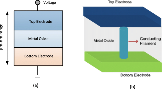
un Esquema de estructura metal-aislante-metal para RRAM. b Vista transversal de RRAM
La aplicación del pulso de voltaje externo a través de la celda RRAM permite una transición del dispositivo desde un estado de alta resistencia (HRS) o un estado APAGADO generalmente referido como valor lógico '0' a un estado de baja resistencia (LRS), o estado ENCENDIDO generalmente referido como valor lógico '1' y viceversa. Se considera que el fenómeno de conmutación resistiva (RS) es la razón detrás de este cambio de valores de resistencia en una celda RRAM. Una RRAM preparada se encuentra inicialmente en el estado de alta resistencia (HRS), para cambiar el dispositivo de HRS a LRS, la aplicación del pulso de alto voltaje permite la formación de rutas conductoras en la capa de conmutación y la celda RRAM se conmuta en un LRS [72]. Este proceso que ocurre debido a la ruptura suave de la estructura metálica del aislante metálico (MIM) generalmente se denomina "electroformado" y el voltaje al que se produce este proceso se denomina voltaje de formación ( V f ). Debe tenerse en cuenta que el voltaje de formación depende del área de la celda [73] y del espesor del óxido [74]. Ahora, para cambiar la celda RRAM de LRS a HRS, el pulso de voltaje denominado voltaje de RESET ( V restablecer ) que permite esta transición de conmutación y el proceso se refiere al proceso "RESET" [75-78]. El HRS de la RRAM se puede cambiar a LRS en la aplicación del pulso de voltaje. El voltaje al que se produce la transición de HRS a LRS se denomina voltaje SET ( V establecer ) y el proceso se denomina proceso "SET" [79]. Para leer de manera eficiente los datos de la celda RRAM, se aplica un pequeño voltaje de lectura que no perturbará el estado actual de la celda para determinar si la celda está en el estado 0 lógico (HRS) o el estado 1 lógico (LRS). Dado que tanto LRS como HRS conservan sus valores respectivos incluso después de la eliminación del voltaje aplicado, RRAM es una memoria no volátil. Dependiendo de la polaridad de la tensión aplicada, la RRAM se puede clasificar en dos tipos de modos de conmutación:(i) conmutación unipolar y (ii) conmutación bipolar [80]. En la conmutación unipolar, la conmutación (proceso de configuración y reinicio) del dispositivo entre varios estados de resistencia no depende de la polaridad del voltaje aplicado, es decir, la conmutación puede ocurrir al aplicar un voltaje de la misma polaridad pero diferente magnitud como se muestra en la Fig. 4a. En la conmutación bipolar, por otro lado, la conmutación (proceso de ajuste y reinicio) del dispositivo entre varios estados de resistencia depende de la polaridad del voltaje aplicado, es decir, una transición de un HRS a LRS, ocurre en una polaridad (positiva o negativo) y la polaridad opuesta cambia la celda RRAM de nuevo al HRS como se muestra en la Fig. 4b. En la conmutación unipolar, el calentamiento Joule se interpreta como el mecanismo físico responsable de romper un filamento conductor durante la operación de reinicio. En la conmutación bipolar, por otro lado, la migración de especies cargadas es la principal fuerza impulsora para la disolución del filamento conductor, aunque el calentamiento Joule todavía contribuye a acelerar la migración. Para garantizar que no haya una ruptura permanente de la capa de conmutación dieléctrica durante el proceso de formación / fraguado de RRAM, una corriente de cumplimiento ( I cc ) se aplica para el dispositivo RRAM. La corriente de cumplimiento ( I cc ) generalmente se asegura mediante un dispositivo de selección de celda (transistor, diodo, resistencia) o mediante un analizador de parámetros de semiconductores durante la prueba fuera del chip.
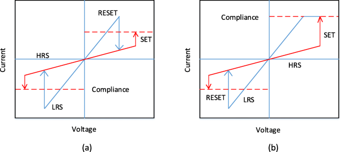
Curvas I-V para RRAM. un Conmutación unipolar y b conmutación bipolar [4]
Mecanismo de conmutación resistiva
La conmutación de la celda RRAM se basa en el crecimiento de filamento conductor (CF) dentro de un dieléctrico. El CF es un canal que tiene un diámetro muy inferior del orden de nanómetros que conecta los electrodos superior e inferior de la celda de memoria. Se obtiene un estado de baja resistencia (LRS) con alta conductividad cuando el filamento está conectado y la alta resistencia (HRS) se obtiene cuando el filamento se desconecta con un espacio entre los electrodos [91]. Según la composición del filamento conductor, la RRAM se puede clasificar en los dos tipos siguientes:(i) RRAM basada en iones metálicos, también conocida como memoria de acceso aleatorio de puente conductor (CBRAM) y (ii) RRAM basada en filamentos de vacantes de oxígeno referida como el 'OxRRAM'. Cabe señalar aquí que CBRAM a veces se denomina memoria de metalización electroquímica (ECM), mientras que "OxRRAM" a veces también se conoce como memoria de cambio de valencia (VCM).
En la RRAM basada en iones metálicos, también denominada "CBRAM", el mecanismo físico responsable de la conmutación resistiva se basa en la migración de iones metálicos y las reacciones posteriores de reducción / oxidación (redox) [92, 93]. La estructura CBRAM consta de un electrodo superior oxidable (ánodo) como Ag, Cu y Ni, un electrodo inferior relativamente inerte (cátodo), p. W, Pt y una capa de óxido metálico intercalada entre los dos electrodos. La formación de filamentos en tales células de memoria se produce debido a la disolución de los electrodos metálicos activos (más comúnmente Ag o Cu), el transporte de cationes (Cu + o Ag + ), y su posterior deposición o reducción en el electrodo de fondo inerte [94]. Por lo tanto, el comportamiento de conmutación resistiva de este tipo de RRAM está dominado por la formación y disolución de los filamentos metálicos.
Para obtener una mejor comprensión del mecanismo de conmutación de CBRAM basado en iones metálicos, consideremos un ejemplo de células Ag / a-ZnO / Pt RRAM [41]. En la figura 5 se muestra una ilustración esquemática general que representa el proceso de conmutación de la celda de memoria de acceso aleatorio de puente conductor. En la figura 5a se representa el estado prístino de la celda de memoria CBRAM. El electrodo superior de Ag (TE) es un componente activo en la formación del filamento, mientras que el electrodo inferior de Pt es inerte. En la aplicación de la polarización de voltaje positivo al electrodo superior de Ag, la oxidación (Ag → Ag + + e - ) ocurre en el electrodo superior debido a que Ag + Los cationes se generan y se depositan en la capa dieléctrica (a-ZnO) del electrodo de Ag. El sesgo negativo en el electrodo inferior de Pt (BE) atrae el Ag + cationes, y como tal, la reacción de reducción (Ag + + e - → Ag) ocurre en el electrodo inferior. Por lo tanto, el Ag + los cationes se reducen a átomos de Ag y se acumulan hasta que se forma el puente conductor (Fig. 5b-d) y se dice que el dispositivo RRAM exhibe LRS. Este proceso se conoce como "SET". Cuando se invierte la polaridad del voltaje aplicado, el filamento altamente conductor se disuelve casi por completo y se dice que el dispositivo está en el estado de alta resistencia (HRS). Este proceso se denomina "RESET" y se muestra en la Fig. 5e.
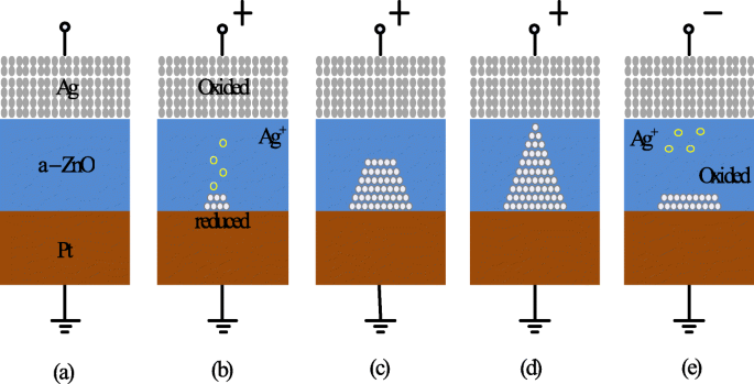
Esquema del mecanismo de conmutación del puente conductor RRAM. un Estado prístino del dispositivo RRAM. b , c Oxidación de Ag y migración de Ag + cationes hacia el cátodo y su reducción. d La acumulación de átomos de Ag y electrodo de Pt conduce al crecimiento de filamentos altamente conductores. e La disolución del filamento tiene lugar al aplicar voltaje de polaridad opuesta [41]
En la RRAM basada en vacantes de oxígeno (OxRRAM), el mecanismo físico responsable de la conmutación resistiva generalmente se asocia con la generación de vacantes de oxígeno ( V \ (_ {o} ^ {2 +} \)) y la posterior reubicación de iones de oxígeno (O 2− ), lo que permite la formación de filamento conductor entre los electrodos superior e inferior de la celda RRAM [59]. Inicialmente, para la celda RRAM tal como se fabrica, es esencial el proceso de formación, es decir, la ruptura suave del dieléctrico. Una vez que se produce la degradación dieléctrica suave, los átomos de oxígeno se eliminan de la red con la aplicación de un campo eléctrico elevado hacia la interfaz del ánodo y se convierten en iones de oxígeno (O 2− ) mientras que las vacantes de oxígeno ( V \ (_ {o} ^ {2 +} \)) quedan en la capa de óxido. Los iones de oxígeno (O 2− ) reaccionan con los materiales del ánodo o se descargan como oxígeno neutro no reticular, si los metales nobles se utilizan como materiales para que el ánodo forme una capa de óxido interfacial. Por tanto, la interfaz electrodo / óxido se comporta como un "depósito de oxígeno" [85]. A continuación, la acumulación de las vacantes de oxígeno ( V \ (_ {o} ^ {2 +} \)) en el óxido a granel cambia la celda RRAM al estado de baja resistencia (LRS) a medida que se forma el filamento conductor (CF) y la corriente apreciable fluye en el dispositivo. Para devolver el dispositivo al estado de alta resistencia (HRS), se produce el proceso de reinicio durante el cual los iones de oxígeno (O 2− ) migran de nuevo al óxido a granel desde la interfaz del ánodo y se combinan con las vacantes de oxígeno ( V \ (_ {o} ^ {2 +} \)) o para oxidar los precipitados metálicos de CF y, por lo tanto, romper parcialmente el filamento, volviendo así la celda RRAM a HRS. Para las células RRAM que exhiben un mecanismo de conmutación unipolar, la difusión de iones de oxígeno (O 2− ) se activa térmicamente por la corriente de calentamiento Joule y, como tal, los iones de oxígeno se difunden desde la interfaz o la región alrededor de la CF debido al gradiente de concentración. Además, debe tenerse en cuenta que se requiere una corriente de reinicio relativamente más alta en RRAM de conmutación unipolar para elevar la temperatura local alrededor de CF. En RRAM de conmutación bipolar, por otro lado, los iones de oxígeno (O 2− ) necesita ayuda del campo eléctrico inverso, ya que la capa interfacial puede presentar una barrera de difusión significativa y la difusión térmica pura no es suficiente. Cabe señalar que la ruptura parcial de la CF se produce en ambos casos, cambiando la celda RRAM al estado de alta resistencia (HRS). Esto se debe principalmente a la formación de vacantes de oxígeno ( V \ (_ {o} ^ {2 +} \)) y una región pobre que resulta en la brecha de túnel para los electrones. Para volver a cambiar el dispositivo al LRS (proceso SET), el CF vuelve a conectar los electrodos como resultado de la ruptura suave en la región del espacio. Un proceso de configuración / reinicio similar puede repetirse durante muchos ciclos.
Basado en la discusión anterior, CBRAM también conocido como memoria de metalización electroquímica (ECM) se basa en un electrodo metálico electroquímicamente activo como Ag, Cu o Ni para formar CF a base de cationes metálicos [95]. La FC en las vacantes de oxígeno RRAM basada en filamentos "OxRRAM", también conocida como memoria de cambio de valencia (VCM), se compone de defectos de vacancia de oxígeno, en lugar de átomos metálicos, debido a la migración de aniones dentro del propio material de almacenamiento [96]. Aunque el mecanismo de conmutación tanto de "OxRRAM" como de "CBRAM" se discute en detalle, todavía hay cierto debate sobre los mecanismos de conmutación de ambos tipos de RRAM [97]. Por ejemplo, dónde comienza a crecer el CF en el proceso de fraguado y dónde interrumpirse en el proceso de reinicio, y cómo estas vacantes de oxígeno / átomos de metal se juntan para formar el CF. Las características de corriente-voltaje (I-V) de 20 ciclos de conmutación consecutivos de Ta / TaO x / Se investigó la estructura de RRAM basada en Pt [98] y se observó la clara variación de LRS y HRS para ciclos de conmutación consecutivos. Como resultado, la ventana de memoria general disminuye, lo que degrada el rendimiento general de RRAM. Esta variabilidad de resistencia de ciclo a ciclo se atribuye principalmente a la formación aleatoria de CF, así como a su ruptura durante la operación de ajuste y reinicio, respectivamente.
En la Tabla 3 se muestra una comparación de OxRRAM con CBRAM basada en varios parámetros operativos [81, 84, 86–88, 99, 100]. Esta comparación revela la sorprendente diferencia en términos de las características de resistencia de estos tipos de memoria RRAM. Esta diferencia se debe a que los filamentos conductores de CBRAM están compuestos principalmente de átomos de metal que son relativamente más fáciles de derivar y difundir en comparación con las vacantes de oxígeno, lo que provoca la degradación del tiempo de retención y las características de resistencia de CBRAM en comparación con OxRRAM. Aunque el mecanismo de conmutación de ambos tipos de RRAM es diferente, existen muchas características comunes entre los dos. La única diferencia significativa es que la resistencia de OxRRAM es significativamente mayor que la de CBRAM.
Métricas de rendimiento de la memoria resistiva de acceso aleatorio (RRAM)
Resistencia
La memoria resistiva de acceso aleatorio implica frecuentes transiciones entre un estado de alta resistencia (HRS) y un estado de baja resistencia (LRS). Cada evento de conmutación entre los estados resistivos puede introducir un daño permanente y causar una degradación del desempeño de la RRAM. Por tanto, la resistencia se define como el número de veces que un dispositivo RRAM se puede cambiar entre HRS y LRS, garantizando al mismo tiempo una relación fiable y distinguible entre ellos [101]. Por lo tanto, una prueba de resistencia determina el número máximo de ciclos de activación / desactivación que pueden conmutarse eficazmente antes de que el HRS y el LRS ya no sean distinguibles. Las características de resistencia de RRAM se obtienen realizando una secuencia de barridos I-V en una celda de conmutación resistiva y la posterior extracción de R HRS y R LRS sobre la aplicación de un voltaje de lectura (típicamente 0,1 V) [41]. Este método es confiable ya que se puede obtener la correcta conmutación del dispositivo en cada ciclo; sin embargo, este método es muy lento porque el tiempo requerido para obtener un barrido I-V puede ser mucho mayor, particularmente si están involucradas las corrientes más bajas.
Los ciclos de resistencia en un H f O x La celda RRAM muestra una fuerte dependencia del tamaño de la celda, como se muestra en la Fig. 6a, en la que se informa una mejor resistencia en el dispositivo RRAM con un tamaño de celda mayor. Además, la reducción vertical del espesor de la capa da como resultado la degradación del rendimiento de resistencia para el voltaje SET a 2,5 V, como se muestra en la Fig. 6b [102]. Esta degradación en el rendimiento de resistencia con la reducción de la capa de conmutación es el resultado del número reducido de iones en la región activa. H f O x RRAM basado en presenta un excelente rendimiento de resistencia de 10 6 ciclos en una matriz de 1 kb con un tamaño de celda de 30 nm por debajo de 0,18 μ m tecnología y lo mismo se muestra en la Fig. 6c [103]. Añadiendo una capa adicional de A l O x por encima del electrodo inferior (BE), la estabilidad de la matriz se puede mejorar aún más a medida que aumenta la inmunidad a las perturbaciones de lectura para HRS. Para T a O x -basado en RRAM, se observó una degradación en el rendimiento de resistencia al aumentar el ancho de pulso y la amplitud del voltaje de RESET en Ta / Ta 2 O 5 / Estructura TiN RRAM [105]. Una comparación del electrodo inferior de TiN y Ru en el Ta / Ta 2 O 5 / TiN RRAM muestra que la principal causa de degradación de la resistencia se debe a la reacción de los iones de oxígeno con el electrodo de TiN. Además, una resistencia mejorada de 10 9 Los ciclos de conmutación se obtuvieron sin verificación en una estructura RRAM similar al reducir el Ta 2 O 5 capa inferior a 3 nm [106] y uso de pulso triangular que tenga <5 ns de ancho. Para el rendimiento de la matriz a gran escala, una comparación de 2-Mb Ta 2 O 5 memoria antes y después de 10 5 Los ciclos de prueba de resistencia se muestran en la Fig. 6d [104]. Las distribuciones de corriente de la celda muestran una pequeña variación para los ciclos inicial y final. Además, la corriente de celda para LRS cae por debajo de 50 μ A, que indica un bajo consumo de energía de la matriz. The resistive switching devices with endurance higher than 10 12 cycles have been reported in different types of RRAM cells involving tantalum oxide (TaO x )-based switching mediums [32, 36, 59]. Thus, tantalum oxide-based RRAM devices seem to be exhibiting the highest endurance.

un Endurance cycles of H f O x -based RRAM at different SET voltage and cell size b with different thickness (T5=2 nm, T20=10 nm) at 2.5 V set voltage. c Resistance distribution of 1-kb array obtained from Weibull plots under different endurance cycles. d 100 k cycles endurance of 2-Mb-Ta2 O 5 -based array; Reprinted from refs [102–104]
Retention
The data retention of a RRAM device involves investigating stability over a period of time for both LRS and HRS after undergoing set and reset transitions. In other words, the time period for which a memory cell will remain in a particular state after the set/reset operation determines the capability of a memory cell to retain its content [11]. The application of the constant voltage stress (CVS) over time using a low read voltage (0.1 V) and the measurement of the current versus time (I-t) curve for both LRS as well as the HRS enables the measurement of state retention. Due to the dispersing nature of atomic rearrangements induced in RRAM because of set voltage, the long retention time in LRS is difficult to obtain whereas, in HRS, retention is not a concern as it is usually the natural state of the device and RRAM will continue to remain in this state if no bias (or low bias) is applied. The retention in the LRS depends on the compliance limit during the SET transition, e.g. in RRAMs based on conductive filament switching mechanism, the larger compliance current produces a stronger conducting filament which is more stable over time [28, 41], as compared to a smaller compliance current. A projected endurance of 10 years at 85 ∘ C has been demonstrated in Ti/HfO2 /TiN [18]. A commonly used method to obtain device endurance is by applying read pulse at high temperature after certain time intervals (e.g. every 1 s) and extrapolate the resistance to a 10-year period. Although this method is easy to implement, it has certain limitations primarily due to the read voltage stress applied to the cell. An alternative method is to change the temperature and record the time until the device fails. Activation energy is extracted by plotting the Arrhenius plot and extrapolate down to the operating temperature. However, the limitation of this method is that waiting is necessary until the failure occurs in the RRAM cell, and thus, this method is more time-consuming and expensive.
The device characteristics of H f O x -based RRAM [81, 103] developed at the Industrial Technology Research Institute, Taiwan, are demonstrated to further understand the working of RRAM device. The transmission electron microscopy (TEM) image of the TiN/Ti/ H f O x /TiN RRAM device with 30-nm cell size is shown in Fig. 7a. The device exhibits bipolar switching characteristics and the I-V curve obtained at 200 μ A set compliance current is shown in Fig. 7b. The device presents endurance of 10 6 switching cycles with the resistance on/off ratio greater than 100 at set/reset programming conditions of + 1.5 V/– 1.4 V pulse with 500 μ s pulse width and the same is depicted in Fig. 7c.

un Transmission electron microscopy (TEM) image of TiN/Ti/HfO x /TiN RRAM device. b Typical current-voltage (I-V) characteristics of the device with 30-nm cell size. c 10 6 endurance switching cycles obtained from 500 μ s pulse. d A retention lifetime of 10 years is expected by testing at 150 ∘ C; reprinted from refs. [81, 103]
Uniformity
In RRAM cell, poor uniformity of various device characteristics is one of the significant factors limiting the manufacturing on a wider scale. The switching voltages, as well as both the HRS and the LRS resistances, are among the parameters exhibiting a high degree of variation. The variations of the resistance switching include temporal fluctuations (cycle-to-cycle) and spatial fluctuations (device-to-device). The stochastic nature of the formation and rupture of conductive filament is believed to be the main reason for these variations. Cycle-to-cycle and device-to-device variability is a major hindrance for information storage in RRAM devices [59]. The observation of cycle-to-cycle variability is influenced by the change in the number of oxygen vacancy defects that arise in the CF due to its stochastic nature of formation and rupture during the switching event [107]. Due to this random nature of the CF, the prediction and the precise control of the shape of the CF becomes extremely challenging. This variability becomes worse as the compliance limit (i.e. compliance current ‘I cc ’) is reduced. On the other hand, for the higher value of ‘I cc ’, the ratio of standard deviation (σ ) and average resistance (μ ) is low, resulting in a smaller LRS resistance spread. This is attributed to the higher defects in the CF, thus forming a well-defined path for current conduction.
RRAM also exhibits device-to-device (cell-to-cell) non-uniformity which also degrades the memory performance by reducing the memory margin between two states. The origin of this variability is attributed to the non-uniformities in the fabrication process such as the thickness of the switching film, etching damages and surface roughness of the electrodes. A lot of research has been conducted to improve the uniformity of RRAM and several methods have been explored for the same. One of the methods utilizes the concept of inserting nano-crystal seeds which confine the paths of the conductive filament by enhancing the effect of local electric field [82, 90, 108]. In Ti/TiO 2−x /Au-based RRAM [28], the induction of platinum (Pt) nano-crystals within the thin TiO 2−x results in an enhanced uniformity of the RRAM cell. The Pt nano-crystals limit the switching effect into regions with high oxygen vacancy generation probability which results in improved uniformity. In another approach, engineering the electrode/oxide interface by embedding appropriate buffer layers is very useful in achieving uniform RRAM operation. In HfO x -based RRAM [109], a thin Al buffer layer is inserted between the TiN electrode and HfO x oxide layer. This results in significant improvement of set voltage distribution as well as the resistance distribution, thus enhancing the uniformity of the device. The improvement in the SET voltage and the resistance distribution of the RRAM device after inserting a thin Al buffer layer between TiN electrode and HfO x bulk oxide and the same is depicted in Fig. 8 [59]. Al atoms are assumed to diffuse into HfO2 thin films, and they tend to localize oxygen vacancies due to the reduced oxygen vacancy formation energy, thus stabilizing the generation of conductive filaments, which helps to improve the resistance switching uniformity.

Uniformity improvement of Al buffered HfO x RRAM compared to HfO x -based RRAM array. un Statistical distribution of SET voltage (V set ) obtained from 100 DC sweep cycles. b HRS and LRS statistical distribution for 100 pulse sweep cycles; reprinted from ref. [59]
In addition to the materials engineering approach, a novel programming method has also been suggested to reduce fluctuations. A multistep forming technique was implemented in W/HfO2 /Zr/TiN [22]-based RRAM to minimize the overshoot current due to the parasitic effects. A multi-step forming technique results in the gradual formation of the filament; thus, a low set/reset current is achieved improving the switching characteristics of the device. Various other methods such as constant voltage forming and hot forming (usually referred to as forming at a higher temperature) have also been investigated to effectively reduce the resistance variations [110]. Another method of achieving high uniformity is by applying a pulse train rather than a single pulse to a RRAM cell [23]. This approach not only results in improved uniformity but also enhances the multilevel capability of a RRAM cell.
Effect of Operating Temperature and Random Telegraph Noise
To achieve a reliable performance of the RRAM device, the effect of operating temperature and random telegraph noise (RTN) is investigated. It is observed that the resistance of both the LRS and HRS states undergoes variations because of the change of operating temperature. The temperature study of TiN/HfO2 /Ti/TiN [111] was carried out. A positive sweep voltage of <3 V magnitude and compliance current of 1 μ A was applied for the electroforming. Once forming takes place, a reset voltage (V reset ) <–1 V switches the device back to the HRS (OFF state). To switch the device back to the LRS (ON state), set voltage (V set ) <1 V is applied.
The reset operation in RRAM device tends to show voltage-controlled negative differential resistance (NDR). The reset operation occurs abruptly at low temperatures, while for temperatures above room temperature, the reset process takes place more gradually. The resistance of the RRAM device in the pristine state, as well as the ON state and OFF state as a function of temperature is depicted in Fig. 9a. The semiconducting behavior is observed for the pristine state as well as the OFF state, i.e. resistance decreases with increase of temperature. For the ON state, a metallic characteristic is observed, i.e. resistance increases with increase of temperature. Due to the variation of resistance with change in temperature, R OFF /R ON also decreases from a value of 20 to approximately 5 over the temperature range of 213–413K. In Ti/HfO x /Pt devices, decrease in R OFF /R ON was observed with temperature-dependent cycling. This decrease in resistance ratio was attributed to the built-up of oxygen-vacancy-related traps inside the HfO2 metal oxide layer [112, 113]. Additionally, temperature-dependent measurements without set/reset operation were carried out to evaluate the impact of I-V cycling on the R OFF /R ON proporción. The sweep voltage across the RRAM device was stopped before reaching V set y V reset valores. For OFF state resistance (green rectangles), a weaker temperature dependence was observed in contrast to the ON state resistance (green circles) which exhibited similar characteristics, compared to the cycling case. From these observations, we infer that I-V cycling induces stronger temperature dependence, which decreases the R APAGADO / R ACTIVADO proporción. The effect of temperature variation on the switching voltages V set y V reset is depicted in Fig. 9b. The slight variation in V set with changing temperature indicates that there is no significant temperature difference. For the case of V reset , the general trend is that a decrease in voltage value of about 0.2 V with temperature increase in the range of 233–333K is observed. Also, a slow increase of V reset is observed for 353–413K temperature range.

The effect of varying temperature on a virgin resistance (left axis) and the OFF-state as well as the ON-state resistances (right axis) at 213–413K temperature range and b switching voltages V set y V reset; reprinted from ref. [111]
Random telegraph noise (RTN) is another factor that affects the performance of RRAM. RTN has for long been used as an indicator of device performance and reliability. RTN decreases the memory margin between the HRS and LRS because of the extensive fluctuations in the read current during the read operation. Due to the effect of RTN, the read margin, scaling potential and the multilevel cell capability of a RRAM cell are greatly affected [114]; thus, it needs to be investigated to achieve reliable performance. To investigate the effect of bottom electrode on RTN, an analysis of Ta2 O 5 / TiO 2 RRAM [115] was carried out. The examples of complex RTN signals in LRS and HRS are depicted in Fig. 10. RTN causes read instability in the RRAM device, thus reducing the read margin, multibit storage implementation and hindering device scaling. The RTN is attributed to the trapping and de-trapping of electrons in the proximity of the CF in LRS whereas it occurs in the tunneling gap in the HRS state. Although the physics of RTN is still not clear and is being highly debated, the electron trapping and de-trapping which temporarily inhibits the charge transport is widely accepted as the mechanism responsible for fluctuation due to RTN. It is observed that with the decrease in operation current, the amplitude of RTN increases, thus highly affecting the HRS level. Therefore, it is necessary to ensure the additional resistance margin to achieve reliable performance. RTN in RRAM has been researched extensively, although the physical mechanism of RTN is still not explicitly defined. RTN can be utilized as a tool to map the movements of active vacancies in RRAM due to its time-dependent variation. This might be quite useful to understand the failure mechanisms of other reliability issues.

Complex RTN signals in LRS and HRS of Ta2 O 5 / TiO 2 -based RRAM depicting normalized noise amplitude and average current; reprinted from ref. [114]
Multilevel Resistive Random Access Memory (RRAM)
Multilevel Per Cell (mlc) Storage
Owing to their small physical size and low power consumption, RRAM devices are potential for future memory and logic applications. Increased storage density is among the most critical aspects of memory technology to enable the design of multibit capacity [89] memory cells. The multiple resistive states can be achieved in RRAM cells which provide benefits of low-cost and high-density non-volatile data storage solutions. Currently, a lot of research is being conducted in the area of RRAM to scale down the dimensions and increase the structural density of memory arrays. Previously, the storage density of RRAM has been increased by the reduction of device size; however, the complexity involved in the experimental procedures limits its successful implementation. Another suggested method is employing three-dimensional (3D) crossbar architectures. Two types of architectures of ‘vertical’ and ‘crossbar RRAM’ have been proposed [116, 117]; however, both these architecture types require advanced fabrication procedures which is not desirable. A much simpler alternative to increase storage density in RRAM devices is by making use of multilevel cell (MLC) storage technology which enables storing more than one bit per cell without reducing the physical device dimensions. This MLC is one of the most promising properties of RRAM which can significantly increase the memory storage density [83, 118–125]. Thus, instead of a single high and low resistance state (HRS and LRS), we can achieve multiple HRS and LRS, without changing the device dimensions. However, to achieve reliable MLC operation, the precise control over the resistance of the different resistance levels of RRAM should be ensured; otherwise, the device will suffer from resistance variability and reliability issues mainly due to the random nature of the conductive filament formation during the switching process [126].
Methods to Obtain Multilevel Per Cell (mlc) Modes in RRAM
The MLC behavior in RRAM makes it very useful for high-density applications. To obtain MLC behavior in RRAM, the following three methods are employed:(i) changing compliance current, (ii) controlling reset voltage and (iii) varying pulse width of program/erase operation.
MLC by Changing Compliance Current
The RRAM device is usually operated with 1-RRAM (1R) cell configuration [41] or in 1-Transistor 1-RRAM (1T-1R) cell configuration [18]. The MLC characteristics in 1R configuration can be obtained by changing the current compliance (I cc ) during ‘set’ operation whereas the MLC characteristics in 1-Transistor 1-RRAM (1T-1R) cell structure are controlled by varying the voltage at the gate of the transistor, which enables the control of compliance current (I cc ) during the set operation of a RRAM cell. The typical MLC I-V curves of Ti/Ta2 O 5 /Pt [127] based RRAM cell are shown in Fig. 11. As the compliance current (I cc ) is increased from 150 μ A to 1 mA, six different LRS are obtained at I cc =150 μ A, I cc =200 μ A, I cc =300 μ A, I cc =500 μ A and I cc =700 μ A, I cc =1 mA due to the increase in the respective current of LRS (I LRS ) while the HRS is maintained constant and the HRS current (I HRS ) remains same for all the LRS levels. For Ti/Ta2 O 5 /Pt RRAM, with the increase in I cc , the maximum reset current (I reset ) also increases while the set voltage is almost maintained constant. Also, it was observed that the resistance of the LRS (R LRS ) decreases while the (I reset ) increases owing to the stronger filament formation with the increase in I cc .

Multilevel characteristics of Ti/Ta2 O 5 /Pt RRAM obtained by controlling the compliance current. ‘Reproduced from [127], with the permission of AIP Publishing’
The formation of the CF and its corresponding widening with an increase in I cc is the attributed mechanism of multilevel per cell (MLC) in compliance current (I cc ) mode as depicted schematically in Fig. 12. With an increase in the size of CF because of an increase of I cc , the resistance of the CF decreases and hence results in multiple LRS levels for different values of I cc . It is also observed that I reset increases with increasing I cc as higher power is required to rupture the CF having larger diameter.

Schematic illustration of multiple resistance states in RRAM cell obtained by varying compliance current ‘I cc ’ [98]
MLC by Controlling Reset Voltage
The MLC characteristics in a RRAM cell can also be obtained by controlling the reset voltage (V reset ) while (I cc ) is maintained constant. In this case, the typical MLC I-V curves of TiN/HfO x /AlO x /Pt-based RRAM cell [128] by applying different (V reset ) of − 2.1 V, − 2.7 V and − 3.3 V are shown in Fig. 13.

Multilevel characteristics of TiN/HfO x /AlO x /Pt RRAM obtained by controlling the reset voltage. ‘Reproduced from [128], with the permission of AIP Publishing’
It is observed that with an increase in (V reset ), the HRS current (I HRS ) decreases; thus, multiple HRS levels with the same LRS resistance are obtained. In addition, the set voltage (V set ) also increases as V reset is increased while as the I reset remains almost constant.
The decrease in I HRS with the increase in reset voltage is primarily due to the increase in the gap between the metal electrode and tip of the CF as depicted in Fig. 14. The more the magnitude of the V reset , the larger the gap and thus the higher the value of resistance. Therefore, an increase in the gap between the CF tip and bottom electrode (BE) with increasing reset voltage results in multiple resistance levels of HRS. It is observed that the devices in which the I reset shows a gradual change in current instead of the abrupt change during the ‘reset’ operation, the change in HRS resistance in such devices can be due to decrease in the size of the conductive filament (CF) as V reset is increased. This approach is more viable practically for cross-point architectures as it requires relatively lower complex circuitry.

Schematic illustration of multiple resistance states in RRAM cell obtained by varying reset voltage ‘V reset ’ [98]
MLC by Varying Program/erase Pulse Width
MLC characteristics can also be obtained by varying the program/erase pulse width while the amplitude of the pulse is maintained constant [23]. In HfO x -based RRAM [128], three HRS levels were demonstrated by varying the width of the reset pulse from 50 ns to 5 μ s. This method of obtaining MLC characteristics in RRAM is relatively easier; however, this scheme is energy inefficient. This drawback limits the application of this method to obtain reliable characteristics in the RRAM cell. The higher energy consumption of the RRAM device was confirmed on the comparison of the transient responses between the reset pulse amplitude and pulse width control. This is particularly due to the higher unwanted energy dissipation as the thermal energy in the resistive switching material.
A summary of RRAM devices exhibiting multiple resistance states is shown in Table 4. As is evident from the table, various RRAM devices with multiple resistance states have been reported. Till date, however, only 8 resistance states have been demonstrated in a single RRAM cell either by varying I cc or V reset . Therefore, there is a huge scope for increasing the number of resistance states in the RRAM cell, thus enhancing its storage density.
Modeling of RRAM Devices
Modeling plays a very critical role in development of devices utilizing semiconductor technologies. To fully understand device operation and to optimize the performance, an accurate model is of great importance. A number of RRAM models with varying features and accuracy have been proposed [129]. This section discusses the characteristics and attributes of the various commonly used RRAM models popular.
Stanford/ASU Model
One of the most popular physics-based RRAM models is the Stanford/ASU RRAM model [130–132], proposed by Guan et al. and Chen et al. This model was applied to validate the I-V switching characteristics of HfO2 RRAM [128] and includes the effect of Joule heating and temperature change on the switching of RRAM devices.
This model is dependent on the CF growth inside a dielectric switching layer. The filament gap, i.e. the gap between the tip of the CF and top electrode, is the internal state variable for this model. The growth of CF inside a dielectric is attributed to the oxygen ion movement and regeneration and recombination of oxygen vacancies [133]. Thus, the rate of change of filament gap (g) is given as [130]:
$$ {\frac{dg}{dt}} =V_{\tiny{0}}.\exp\bigg({{\frac{-E_{a},m}{k_{b}.T}} }\bigg). {\text{Sinh}} \bigg({\frac{qa_{h}\gamma V}{L.k_{b}.T}}\bigg) $$ (1)donde E a is the activation energy, V is the magnitude of the voltage applied across the device, L is the switching material thickness, a h is the hopping distance, γ is the local field enhancement factor, V 0 is the velocity containing attempt to escape frequency, K b is the Boltzmann constant, q is the elementary unit charge and T is the temperature of the conductive filament.
The spatial variation in the gap size is accounted for in this model, in addition to the variations which arise due to the stochastic property of the ion process. A noise signal is added to the gap distance to account for these variations as [130]:
$$ g_{|t+\Delta t} =F \Big[ g_{|t}, {\frac{dg}{dt}} \Big] + \delta_{g}\times\tilde{X}(n)\Delta t, n ={\frac{t}{T_{GN}}} $$ (2)donde Δ t is the simulation time step, the function F represents time evolution of gap size fromt to Δ t. \(\tilde {X}\)(n) is a zero mean Gaussian noise sequence. T GN is the time interval after which \(\tilde {X}\)(n ) changes to next random value.
The variation in the gap size δ g depends on kinetic energy of ions and filament temperature as [130]:
$$ \delta_{g} (T) ={\frac{\delta^{\tiny{0}}_{g}}{\bigg\{ 1+\exp \Big({\frac{T_{\text{crit}}- T}{T_{\text{smith}}}} \Big) \bigg\}}} $$ (3)where \(\delta ^{0}_{g}\) and T smith are fitting coefficients to match the resistance distribution curves to experiments and T crit is a threshold temperature above which the gap size changes significantly.
This model shows strong dependence on temperature; thus, there is a need to account for the change of ‘T’ . With change in cell characteristics, the dynamic inner domain temperature T changes significantly, while the outer domain assumed to be at uniform and stable temperature (T bath ), is related as [130]:
$$ c_{p} {\frac{dT}{dt}} =V(t).I(t) - k(T-T_{\text{bath}}) $$ (4)where C p is the effective heat capacitance of inner domain, V (t) I (t) represents the Joule heating and k is the effective thermal conductivity.
Using a generalized conduction mechanism, the current conduction is defined as [130]:
$$ I(g,v) =I_{\tiny{0}}.\exp\bigg({{\frac{-g}{g_{\tiny{0}}}} }\bigg){\text{Sinh}} \bigg({\frac{V}{V_{\tiny{0}}}}\bigg) $$ (5)donde yo 0 , g 0 y V 0 are the fitting parameters to match experimental results.
One of the significant features of this model is its implementation in neuromorphic applications and RRAM synaptic device design [134], giving the model a great degree of flexibility and further scope for implementation in various neuromorphic systems.
Physical Electro-thermal Model
Physical electro-thermal model was developed by Kim et al. [135] and implemented with tantalum pentoxide (Ta2 O 5 ) -based bilayer RRAM [136–138]. This physical model solves the differential equations based on finite element solving method. This model also makes use of electrothermal physics phenomenon approach for modeling [139], thus giving it advantage in terms of flexibility to incorporate finite element method (FEM) solver to simulate the system very accurately. However, the drawback of this approach is its difficulty in implementation for SPICE and Verilog circuit solvers.
This model describes CF as a doped region having oxygen vacancies as dopants with CF extending from the top to the bottom electrode of the device. To describe the drift-diffusion of vacancy migration, this model assumes the same equation can be used to describe both the processes of oxygen ions and vacancies. The ion model by Mott and Gurney [140] is employed here to describe the process given as [135]:
$$ {\frac{dn_{D}}{dt}} =\Delta \times \bigg(D_{s}.\Delta_{n\tiny{D}}- \mu v n_{D} \bigg) + G $$ (6)donde D s describes the diffusion process, v gives the drift velocity of vacancies and G is the CF growth rate which actually describes the SET process. The parameters are defined as [135]:
$$ D_{s} ={\frac{1}{2}} \times a^{2} \times f_{e} \times \exp \bigg({\frac{- E_{a}}{k_{B}T}} \bigg) $$ (7) $$ v =a_{h} \times f \times \exp \bigg({\frac{- E_{a}}{k_{B}T}} \bigg) \times {\text{Sinh}} \bigg({\frac{q a_{h}E}{k_{B}T}} \bigg) $$ (8) $$ G =A \times \exp \bigg({\frac{- (E_{a}-ql_{m}E)}{k_{B}T}} \bigg) $$ (9)where l m is the mesh size.
These equations govern the physical transformation of the device during SET and RESET transition, thus essentially controlling the CF growth and rupture.
Huang’s Physical Model
Huang’s physical model developed by Huang et al. [141, 142] is a very comprehensive physical model for RRAM device as it takes into account both the CF width and the gap of filament to electrode as the factors affecting the state variable dynamics. In addition, temperature distribution is also accounted for in this model.
SET/RESET process is considered as a result of generation/recombination process of oxygen ions (O 2− ) and oxygen vacancies (V 0 ). During the SET process, CF starts to evolve from the tip of the top electrode (T.E) and elongates in radius with increase in voltage, resulting in final width ‘W’ of the C.F. This model assumes symmetrical cylindrical shape of the C.F. During RESET process, CF ruptures starting from TE till it dissolves completely with increase in voltage. The filament gap distance ‘x’ is defined as the gap between active electrode layer (T.E) and the tip of the C.F.
Thus, for the SET process, parameter ‘W’ acts as state variable, while for RESET, parameter ‘x’ acts as state variable. Therefore, \(\frac {dx}{dt}\) and \(\frac {dw}{dt}\) define the dynamics of the device during the SET/RESET transition.
During the first reset process, CF reduction rate, i.e. release of O 2− , is by the electrode is expressed as [142]:
$$ {\frac{dx}{dt}} =a \times f\times \exp \bigg({\frac{- E_{i}-\gamma Z_{e}V}{k_{B}T}} \bigg) $$ (10)For O 2− hopping within the oxide layer, the CF reduction rate with ‘a’ being the distance between two V0 is given as [142]:
$$ {\frac{dx}{dt}} =a \times f\times \exp \bigg({\frac{- E_{h}}{k_{B}T}} \bigg) {\text{Sinh}} \bigg({\frac{ a_{h}Z_{e}E}{k_{B}T}} \bigg) $$ (11)For the case of RESET process when dominated by recombination between O 2− and V0 is expressed as [142]:
$$ {\frac{dx}{dt}} =a \times f\times \exp \bigg({\frac{- \Delta E_{r}}{k_{B}T}} \bigg) $$ (12)In the initial step of the SET process dominated by recombination of oxygen vacancies with thin CF initially grown is given by [142]:
$$ {\frac{dx}{dt}} =-a \times f_{e}\times \exp \bigg({\frac{- E_{a}-\alpha_{a} Z_{e}E}{k_{B}T}} \bigg) $$ (13)Here, Z and α g are the fitting parameters.
For the second step, CF grows along its radial direction and is defined as [142]:
$$ {\frac{dw}{dt}} =\bigg(\Delta w + {\frac{\Delta w^{2}}{2w}} \bigg) \times f_{e}\times \exp \bigg({\frac{- E_{a}-\gamma Z_{e}v}{k_{B}T}} \bigg) $$ (14)The current flowing through the device is modeled as a correlation of hopping current with voltage and gap distance expressed by [134] as:
$$ i =i_{0}. \exp \bigg({\frac{-x}{x_{T}}} \bigg) {\text{Sinh}} \bigg({\frac{v}{v_{T}}} \bigg) $$ (15)This model is validated in HfO x /TiO x system [141, 142], and a pretty accurate match between the experimental and simulation results is obtained. Although this model accounts for the significant processes which affect the RRAM operation, however, it has some limitations. The most critical one is being incompatible with the SPICE and Verilog-A.
Filament Dissolution Model
This model was developed exclusively for unipolar RRAM devices by Russo et al. [143–145], however was later modified for bipolar RRAM devices [139, 146] also. Filament dissolution model is based on rupture of CF under the effect of significant temperature change caused due to Joule heating.
One of the significant advantages of this model is that it utilizes the simple partial differential equations to account for the device current and temperature changes due to Joule heating as well as the dissolution velocity. The conduction of current within the device is described by Poisson’s equation [144] as:
$$ \triangledown \times \bigg({\frac{1}{\varphi}\triangledown_{v}} \bigg) =0 $$ (16)Here, φ is the oxide resistivity and v defines the electric potential due to the application of external bias voltage to one of the electrodes while the other electrode is connected to ground.
The CF is divided into a number of mesh grids and at each point of the mesh grid the temperature is calculated to describe the rupture of CF. The Fourier steady-state heat equation describes this effect as [144]:
$$ -\triangledown \times \bigg(k \triangledown T \bigg) =\varphi J^{2} $$ (17)donde k represents the oxide layer thermal conductivity, J is the current density and T is the device temperature.
The temperature ‘T’ of the device increases to the critical temperature, after which the device is reset and the CF dissolution takes place. The dissolution factor is modeled as [144]:
$$ V_{\text{DIS}} =V_{\text{DIS}-F}. \exp \bigg({\frac{- E_{a}}{k_{B}T}} \bigg) $$ (18)donde E a is the activation energy, k b is the Boltzmann constant, V DIS−F is a fitting parameter and V DIS is velocity of CF boundary towards symmetry axis.
The resistivity of CF is temperature-dependent and is described as [144]:
$$ \varphi_{\text{CF}} (T) =\varphi_{\mathrm{CF-RT}} \Big[ 1 + C (T-T_{0}) \Big] $$ (19)donde C is the experimentally calculated temperature coefficient of resistivity and φ C F −R T is the standard CF resistivity at room temperature.
COMSOL Multiphysics Software [147] is used for solving the coupled equations for this RRAM model due to its multiphysics capabities and ability to handle such simulations.
Bocquet Bipolar Model
Bocquet bipolar model [148] describes the bipolar oxide-based resistive switching memories utilizing a physics-based modeling approach. Bocquet bipolar model describes the electroforming process of RRAM device, inaddition to utilizing some of the characteristics from Bocquet unipolar model [149] and modifies them significantly according to the bipolar switching characteristics. In this model, the radius of the CF is the internal state variable which effectively governs the switching rate.
To model the electroforming stage, Bocquet bipolar model utilizes electroforming rate (τ Form ) which details the mechanism of conversion to switchable sub-oxide from pristine oxide. The electroforming stage is modeled as [148]:
$$ \tau_{\text{form}} =\tau_{\text{form}0} \times \exp \bigg({\frac{E_{a\text{Form}}-q \times \alpha_{s} \times V_{\text{cell}}}{k_{B}\times T}} \bigg) $$ (20) $$ {\frac{dr_{\text{CFmax}}}{dx}} ={\frac{r_{\text{work}}-r_{\text{CFmax}}}{\tau_{\text{form}}}} $$ (21)donde E a Form is the activation energy for electroforming, τ form0 is the nominal forming rate, α s is the charge transfer coefficient, V cell is the voltage applied between the top and bottom electrodes, r CF is the radius of CF which varies from 0 to r CFmax , q is the elementary charge of electron, T is the temperature of the device and k B is the Boltzmann constant.
The electrochemical redox reaction derived from Butler-Volmer equation [150] is used to describe the SET/RESET operation as [148]:
$$ \tau_{\text{Red}} =\tau_{\text{Redox}} \times \exp \bigg({\frac{E_{a}-q \times \alpha_{s} \times V_{\text{cell}}}{k_{B} \times T}} \bigg) $$ (22) $$ \tau_{Ox} =\tau_{\text{Redox}} \times \exp \bigg({\frac{E_{a}+q \times (1 - \alpha_{s}) \times V_{\text{cell}}}{k_{B} \times T}} \bigg) $$ (23)Aquí, τ Red y τ Ox are the reduction and oxidation rates, respectively. τ Redox is the effective reaction rate considering both reduction and oxidation reactions.
The switching rate is obtained by coupling the above two equations as [148]:
$$ {\frac{dr_{CF}}{dt}} ={\frac{r_{\text{CFmax}}-r_{\text{CF}}}{\tau_{\text{red}}}} - {\frac{r_{\text{CF}}}{\tau_{\text{Ox}}}} $$ (24)Bocquet bipolar model is a quite comprehensive model as it includes the temperature effects as well. The local filament temperature is coupled using heat equation and is given in Eq.(25), the temperature considering a cylindrical-shaped filament is given in Eq. (26). The maximum temperature reached into CF at x =0, the middle of the filament is given in Eq. (27) and the equivalent electrical conductivity in the work area (σ eq ) is given in Eq. (28).
$$ \sigma_{x} \times F(x)^{2} =- k_{th}.{\frac{d^{2}T(x)}{dx^{2}}} $$ (25) $$ T(x) =T_{\text{amb}}+{\frac{V^{2}_{\text{cell}}}{2. L^{2}_{x}.k_{th}}} \bigg({\frac{L^{2}_{x}}{4}- x^{2}} \bigg) \sigma_{eq} $$ (26) $$ T =T_{\text{amb}}+{\frac{V^{2}_{\text{cell}}}{8. k_{th}}} \sigma_{eq} $$ (27) $$ \sigma_{eq} =\sigma_{CF}.{\frac{r^{2}_{\text{CF}}}{r^{2}_{\text{work}}}} - \sigma_{Ox}. {\frac{r^{2}_{\text{CFmax}}-r^{2}_{\text{CF}}}{r^{2}_{\text{work}}}} $$ (28)where (σ x ) is the local electrical conductivity, F ( x ) is the local electric field, σ CF is the electrical conductivity of the conductive filament, k th is the thermal conductivity and T amb is the ambient temperature.
It must be mentioned here that temperature increases with increase in radius of the CF, resulting in self-accelerated reaction due to a positive feedback loop. The self-limited reaction also referred to as SOFT reset [151], on the other hand, occurs due to the decrease in temperature and radius of the CF during RESET operation.
The total current flowing in OxRRAM is the sum of currents flowing in the conductive area (I CF ), the conduction through switchable sub-oxide (I sub−oxide ) and conduction through unswitched pristine oxide (I pristine ). The total current is as [148]:
$$ I_{\text{cell}} =I_{\mathrm{sub-oxide}} + I_{\text{CF}} + I_{\text{Pristine}} $$ (29) $$ I_{\text{CF}} =F.\pi. \sigma_{CF}.r^{2}_{CF} $$ (30) $$ I_{\mathrm{sub-oxide}} =F.\pi. \sigma_{Ox}. \big(r^{2}_{\text{CFmax}}- r^{2}_{CF}\big) $$ (31) $$ I_{\text{Pristine}} =S_{cell}.A.F^{2}. \exp {\frac{-B}{F}} $$ (32) $$ A ={\frac{m_{e}.q^{3} }{8\pi.h.m^{ox}_{e}.\phi_{b} }} $$ (33)The parameter B e is the metal-oxide barrier height (ϕ b )-dependent and is given as [148]:
$$ if \phi_{b}\geq qL_{x}F:B_{e} ={\frac{8 \pi \sqrt{2m^{ox}_{e} }}{3\times h\times q}} \Big[ \phi^{{\frac{3}{2}}}_{b}- (\phi_{b}-qL_{x}E)^{{\frac{3}{2}}} \Big] $$ $$ \text{otherwise}, B_{e} ={\frac{8 \pi \sqrt{2m^{ox}_{e} }}{3\times h\times q}} \times \phi^{{\frac{3}{2}}}_{b} $$ (34)where m e and \(m^{ox}_{e}\) are the effective electron masses into the cathode and oxide respectively, F =\(\frac {V_{\text {cell}} }{L_{x}}\) is the electric field across the active layer, h is the Planck constant and S cell is the section of the RRAM cell.
Discrete solutions are required to implement the model in an electrical simulator. This model accounts well in that aspect, making it suitable for simulation involving electrical circuits. This model implements equations in Eldo circuit simulator [152]. The discrete solutions are given as [148]:
$$ r_{\text{CFmax}_{i+1}} =\big(r_{\text{CFmax}_{i}}- r_{\text{work}} \big) \times e^{ {\frac{-\Delta t}{{\tau}_{\text{form}}}} } + r_{\text{work}} $$ (35) $$ r_{CF_{i+1}} =\bigg(r_{CF_{i}}- r_{\text{CFmax}_{i}} \times {\frac{\tau_{eq}}{\tau_{\text{Red}}}} \bigg) \times e^{ {\frac{-\Delta t}{{\tau}_{eq}}} } + r_{\text{CFmax}_{i}} \times {\frac{\tau_{eq}}{\tau_{\text{Red}}}} $$ (36) $$ \text{where} { \tau_{eq}} =\frac{\tau_{\text{Red}}\times \tau_{\text{Ox}} }{\tau_{\text{Red}}+\tau_{\text{Ox}}} $$ (37)This model has been verified against electrical characterization from an HfO2 -based system [153]. An important feature of this model is that it can account effectively for device to device variability [154, 155]. One of the major limitations of this model is the lack of current or voltage threshold.
This section presents in detail various characteristics and features of the RRAM models. A comparative analysis of the RRAM models discussed in this work is presented in Table 5.
Applications of RRAM
RRAM is seen as one of the standout candidates among the emerging memory technologies that has the potential for reforming the memory hierarchy primarily due to its high speed, the capability of non-volatile data storage, enhanced storage density and logic computing function. The various novel applications of RRAM are discussed in this section.
>Non-volatile Logic
The instruction codes and the data are transferred by making use of buses between various units in a computer system having von Neumann architecture because of the separate computing and memory unit. This data transferring process results increased energy consumption and time delay, which is commonly referred to as ‘von Neumann bottleneck’. For reducing the impact of von Neumann bottleneck [156], the computing process which utilizes RRAM crossbar array is suggested which alters the memory and computing operations in the same core. In addition, to obtain high integration density and low cost [157], two-terminal compact device structure of RRAM and its 4F 2 array architecture are highly beneficial. For example, to obtain simple Boolean logic functions such as ‘logic NOT’, ‘logic AND’, and ‘logic OR’, we require multiple transistors and each single transistor takes 8−10F 2 área. These logic functions can be realized by making use of two or three RRAM cells, resulting in total approximate area of around 10F 2 only [158].
Till date, several methods have been suggested for realizing Boolean logic functions [159, 160]. Boolean computing is significantly more established compared to existing non-Boolean computing paradigms such as neuromorphic computing and quantum computing. Therefore, energy and cost-efficiency of CPU or MCU can be enhanced without the need to develop new algorithms or software, although there is still a lack of technical solution on how to implement complex computing tasks in a crossbar array. Thus, most of research to date focusses on only basic logic level demonstration as it becomes quite complex to implement a whole computing unit using RRAM array.
Neuromorphic Computing
To overcome ‘von Neumann bottleneck’, one of the effective ways is brain-inspired neuromorphic computing which has shown promising potential in a wide range of complex and cognitive tasks like visual/audio recognition, self-driving, and real-time big-data analytics. Compared to CMOS-based neuromorphic network, neuromorphic computing based on RRAM-array offers advantages in terms of on-chip weight storage, online training, and scaling up to much larger array size [161–163]. In addition, the processing speed of RRAM improves by three orders of magnitude, whereas the power consumption rate is reduced by four orders of magnitude [164].
For realizing hardware-implemented neuromorphic computing paradigms, two methods are suggested:one among the strategies mimics the structure and working mechanism of biological neural networks while the other method works on accelerating the existing artificial neural network (ANN) algorithms. In a neural network, a synapse is used to transfer spikes between different neurons in addition to storing information about the transferring weights. The information regarding weights can be acquired through certain learning rules such as spike-time-dependent plasticity (STDP) and spike-rate-dependent plasticity (SRDP) [165–167]. Although some of the works reported in the literature have tried to emulate such learning rules on RRAM devices, it is however quite complicated to extend such types of bioinspired learning rules to a complex task as the theoretical algorithm is still lacking.
A practically viable approach is to map an ANN to a RRAM-based neuromorphic network directly. Some advanced tasks such as pattern and speech recognition have been demonstrated based on this method [166–169]. Although very promising, RRAM-based synapse is still far from being applied as various issues such as material optimization, variation suppressing, control circuit design, architecture, and algorithms design for analog computing need to be addressed effectively.
Security Application
The security aspect has become more prominent with rapid developments in the field of information technology; thus, there is a need for hardware-based security-integrated circuits. In contrast to security circuits based on CMOS logic which exploits the random nature of the semiconductor manufacturing process, security circuits based on RRAM are more robust to attacks of various types due to its completely random switching mechanisms [170, 171]. It must be noted that for security applications, larger variation of RRAM device parameters such as random telegraph noise (RTN), resistance variations and probabilistic switching is desirable, which is quite different from memory applications that require a smaller degree of variation among numerous parameters.
A novel security feature commonly referred to as physical unclonable function (PUF) [172], based on RRAM is proposed for device authentication (strong PUF) and key generation (weak PUF) applications. Significantly larger number of input-output pairs [also called challenge-response pair (CRP) are required for strong PUF, while only a small amount of CRPs of extremely higher reliability are required for weak PUF [173]. Although, PUFs based on RRAM have demonstrated remarkable performance; however, still more practical demonstrations and further evaluations are required to work out the maturity of this new primitive within the field of hardware security.
Non-volatile SRAM
Volatile memory technologies like SRAM and DRAM may consume over half of the static power within the current mobile SoC chips. Thus, to attain fast parallel memory operations, reduced area and low-energy consumption, RRAM-based non-volatile SRAM (nvSRAM) was proposed [174] in which two RRAM cells are stacked on eight transistors, forming an 8T2R structure. Also, non-volatile ternary content-addressable memory (TCAM) having 4T2R cell structure [175] and non-volatile flip flops having reduced stress time and write power based on RRAM have been demonstrated recently [176].
Challenges and Future Outlook
During the past several years, research in the field of emerging memory technologies has grown significantly and several prototype RRAM products have been developed demonstrating the potential for high-speed and low-power embedded memory applications. RRAM is one of the most promising memory technologies because of the advantages of simple structure, compatibility with the existing CMOS technology, good switching speed and ability to scale to the smallest dimensions. As a matter of fact, currently the Flash memory technology is facing difficulties to reduce to lower dimensions and as such RRAM is emerging as a potential replacement especially for fast operation and medium size storage density memory applications.
One of the most critical aspects that needs to be thoroughly investigated is that of the reliability of RRAM. A mechanism must be developed to ensure the detection of the operation failure of the device. Also designing circuits, e.g. a test element group (TEG) design for robust signal sensing, is one of the critical challenges for the emergence of RRAM devices. To achieve high-density memory operation in RRAM, the 1D1R operation is essential. This can be realized by operating the RRAM device in the unipolar mode. However, in the unipolar operation, higher current is needed for the reset process as compared to that of the bipolar operation. This is due to the fact that thermal effect plays a significant role in the unipolar reset process. Thus, to realize a high-density 1D1R RRAM array, the thermal effects both inside and outside a memory element needs to be considered. Also note that till date, in a single RRAM device, no technology has simultaneously reported fast switching, low power, and stable operation. Although, the endurance of RRAM has been reported as high as 10 12 [59], it is still not enough to be able to replace DRAM. The RRAM possesses the switching speed fast enough for DRAM replacement and the materials used in the fabrication for RRAM are very similar to that of DRAM, it becomes a critical challenge to improve the endurance characteristics of RRAM. To improve the endurance characteristics, it is necessary to control the oxygen movement between the electrode and the oxide layer at the interface. It is suggested to insert the second metal layer at the interface which can be easily oxidized and acts as an oxygen reservoir to prevent oxygen from penetrating into the electrode during the resistance switching. The most critical challenge hindering RRAM development till date is the proper understanding of the device switching mechanism which is since long being debated by researchers across the globe. The inconsistent switching mechanism of various reported RRAM devices is believed to be because of variation in the fabrication process, and thus, more rigorous analysis is needed in the future for obtaining a better understanding of the switching mechanism of RRAM devices. The aforesaid issues need to be handled effectively before implementing RRAM in future memory applications. Although, RRAM is highly attractive for use in neuromorphic computations, the biggest challenge to industrialize RRAM lies in its ability to tackle the variability issues, not only at nominal operating conditions but also at high temperatures before they can be used in a wide variety of applications.
Conclusion
This review article provides a brief introduction into the advancement of the memory architecture, the current trends and the limitations while providing a valuable insight into the field of emerging memory technologies. A detailed discussion, highlighting the importance of RRAM, its structure, working mechanism, and classification, has been presented. The key performance parameters and their effect on the RRAM operation has also been detailed within the current manuscript. An elaborate study on the MLC capability of RRAM, along with the methodology have been presented. The manuscript also discusses the important features of the widely accepted RRAM models. The implementation of RRAM for various important applications such as non-volatile logic, neuromorphic computing, security, and non-volatile SRAM have been highlighted. Although, significant success has been achieved in RRAM technology; however, more work is needed as RRAM still suffers from various challenges in terms in terms of high operation current, lower resistance ratios, and reliability issues. More efforts in research should aim to develop methods to achieve faster programming/erasing, lower power consumption, enhancing the storage density by implementing multilevel storage capability and improvement in the fabrication process for enhanced uniformity. In addition, renewed focus should be towards use of RRAM in embedded memory and non-volatile logic applications as breakthroughs in these fields are much more exciting and significant. With continued work and improvements, it is imperative that RRAM devices will be a standout technology for future non-volatile memory applications.
Disponibilidad de datos y materiales
No aplica.
Abreviaturas
- RRAM:
-
Memoria resistiva de acceso aleatorio
- MLC:
-
Multilevel cell
- RTN:
-
Random telegraph noise
- DRAM:
-
Dynamic random access memory
- SRAM:
-
Static random access memory
- PCM:
-
Phase change memory
- STT-MRAM:
-
Spin-transfer torque resistive random access memory
- LRS:
-
Low resistance state
- HRS:
-
High resistance state
- MTJ:
-
Magnetic tunneling junction
- MIM:
-
Metal-aislante-metal
- MoM:
-
Metal-oxide-metal
- PLD:
-
Pulse laser deposition
- ALD:
-
Deposición de la capa atómica
- V set :
-
Set voltage
- V reset :
-
Reset voltage
- V f :
-
Forming voltage
- I CC :
-
Compliance current
- CBRRAM:
-
Conductive bridge resistive random access memory
- OxRRAM:
-
Oxygen vacancies resistive random access memory
- ECM:
-
Electrochemical metallization memory
- VCM:
-
Valence change memory
- CF:
-
Conductive filament
- BE:
-
Electrodo inferior
- TEM:
-
Microscopía electrónica de transmisión
- I-V:
-
Corriente-voltaje
- 1T-1R:
-
1-Transistor 1-RRAM
- ANN:
-
Artificial neural network
- STDP:
-
Spike-time-dependent plasticity
- SRDP:
-
Spike-rate-dependent plasticity
- PUF:
-
Physical unclonable function
- CRP:
-
Challenge-response-pair
- nvSRAM:
-
Non-volatile SRAM
- TCAM:
-
Ternary content addressable memory
- TEG:
-
Test element group
Nanomateriales
- 13 tipos de materiales refractarios y sus aplicaciones
- Mejora del rendimiento y la seguridad en los wearables de IoT
- Cervoz:elegir el almacenamiento flash adecuado para aplicaciones industriales
- Características de conmutación resistiva bipolar de dispositivos RRAM con estructura de tres capas de HfO2 / TiO2 / HfO2 en sustratos recubiertos de Pt y TiN fabricados por deposición de capa atóm…
- Memoria resistiva ZrO2 / ZrO2 - x / ZrO2 sin cumplimiento con comportamiento de conmutación multiestado interfacial controlable
- Una SRAM 4T integrada de RRAM con carga de conmutación resistiva autoinhibida mediante un proceso lógico CMOS puro
- Mecanismo de conducción y resistencia mejorada en RRAM basado en HfO2 con tratamiento de nitruración
- Un estudio colectivo sobre modelado y simulación de memoria resistiva de acceso aleatorio
- Nanowebs grafíticos jerárquicamente macroporosos que exhiben un rendimiento de almacenamiento de carga estable y ultrarrápido
- Síntesis y rendimiento del supercondensador de compuestos de carbono mesoporoso ordenados con polianilina / dopado con nitrógeno
- Un estudio de la variabilidad en la memoria de acceso aleatorio resistivo de contacto por modelo de vacante estocástico